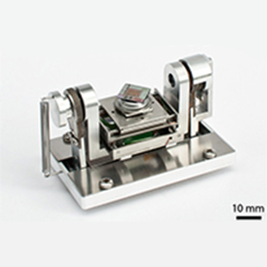
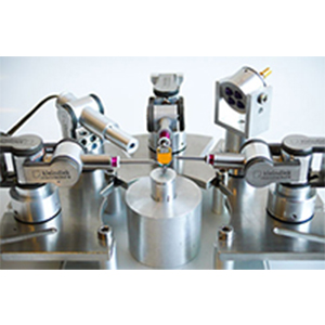
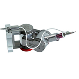
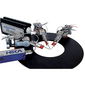
Using a compact nanoprobing setup comprising eight probe tips attached to piezo-driven micromanipulators, various techniques for fault isolation are performed on 28 nm samples inside an SEM. The employed techniques include nanoprobing as well as EBAC. The recently implemented Current Imaging technique is used to quickly image large arrays of contacts providing a means of locating faults. In this case, Current Imaging provides insight into the sample’s behaviour yielding qualitatively comparable results to the more cumbersome cAFM technique. While the results of the TEM investigations including EDX mappings were inconclusive, the Current Imaging technique clearly shows that the root cause is located below the SiGe layer. By combining these techniques inside a FIB/SEM microscope, it is possible to locate and characterize a failure as well as prepare a TEM lamella for further investigation without the necessity to switch to a different tool.