Description
- About
- Advantages
- Specifications
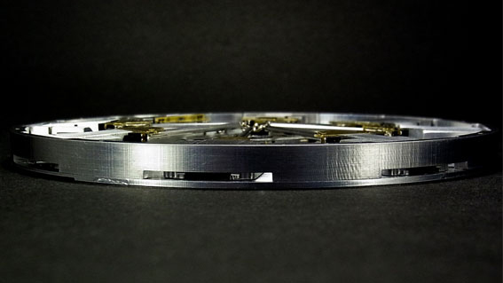
The PS8 Prober Shuttle is already the most compact and highly integrated nanoprobing system in the market. Nonetheless, we found a way to add positional encoders to the platform. This latest feature enables fast and efficient nanoprobing workflows.
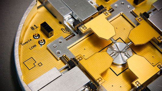
The ability to automatically pre-align the probes is especially important for probing on the most recent technology nodes where beam sensitivity is an issue and thus, very low acceleration voltages are required. Using pre-defined alignment positions, all eight probes can be brought from their individual parked positions into close vicinity to each other at a consistent height above the sample - at the click of a button! This eliminates the tedious pre-alignment task which involved constant corrections of the astigmatism and/or necessitated switching to higher acceleration voltages.
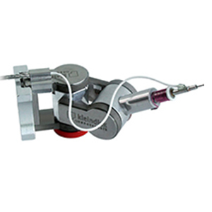
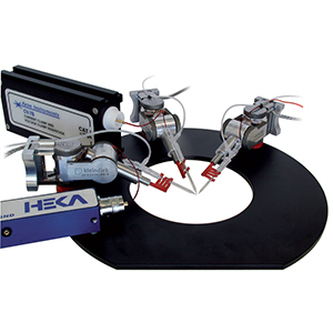
The PS8e utilizes the MM4 ultra-flat three-axis manipulators that exhibit unmatched stability and precision. The entire height of the system is 10 mm, making it compatible with a wide range of SEM load-locks and thus helping you to achieve a higher sample throughput. The Prober Shuttle also offers low-current, low-capacity measurement capability and is fully compatible to the Advanced Probing Tools hardware and software suite including the Live Contact Tester and Electron Beam Induced Current Imaging modules, among others.
Compact & flexible
- Small and practical
- Plug-and-play system with modular components
- Interfacing solutions for most SEM/FIB instruments (including load-lock compatibility)
- Fast setup and removal
- Pioneering cabling technology
- Non-magnetic design for use with immersion lenses
- Lightweight platform is simply placed on your SEMs sample stage
- Can be tilted to FIB angle e.g. for circuit edit or delayering applications
- Easy to retrofit to existing tools
Clear & simple
- Intuitive control interfaces and software
- User-friendly and easy to learn
- Quick and easy probe tip exchange
- Compact, stand-alone electronics
- Effortless work with multiple manipulators
Robust & stable
- Excellent stability
- Low drift (1 nm/min)
- Reliable operation (one year endurance test)
- Virtually insusceptible to vibrations
Fast & precise
- High operating velocity (up to 10 mm/sec)
- Sub-nanometer resolution (0.05 nm)
- No backlash or reversal play
- Extensive working range
- Coarse and fine displacement in one drive
- Fast pre-positioning at the click of a button
Overview
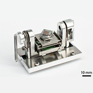
- Total height: 10 mm
- Total width: 140 mm
- Maximum sample area: 20 mm x 20 mm
- Maximum sample height: 20 mm - depending on the sample area and load lock dimensions
- Weight: 200 g + SEM/FIB dovetail
- Clean cable management from flange to rack
- Non-magnetic design
- Ready for 5 nm and beyond
Next generation micromanipulators
A = left / right B = up / down C = in / out
- Operating range: A = 5 mm, B = 90°, C = 5 mm
- Resolution: A < 0.05 nm, B < 0.5 nm, C < 0.05 nm
- Low drift: 1 nm/min
Encoder features
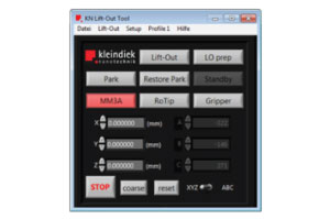
- Park & restore probes with a click of a button
- Drive substage to pre-defined locations
- Fast cycle time
- Automatic tip pre-alignment allows lowkV workflows
Low-capacity, low-current measurements
- Noise: 25 fA @ 1 Hz
- Insulation leakage current: <50 fA/V
- Signal conductor resistance: <5 Ω
- Maximum voltage: 100 V
- Maximum current: 100 mA
All technical specifications are approximate. Due to continuous development, we reserve the right to change specifications without notice.